Littelfuse Gate Drivers Offer Solutions for High-Power Designs
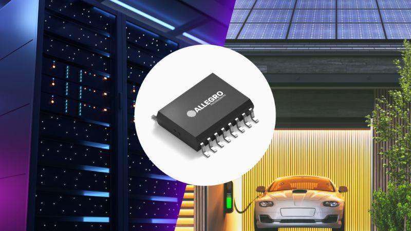
Littelfuse has introduced the IX3407B, a single-channel, galvanically isolated gate driver designed for motor drives, inverters, and other high-voltage power electronics. The company is positioning the part as a replacement for optocoupler or transformer-based interfaces for designers with aggressive common-mode transients and tight timing at elevated dv/dt.

The IX3407B isolated gate driver. Image used courtesy of Littelfuse
IX3407B Specs
The IX3407B drives power switches through independent source (OUT+) and sink (OUT-) pins that each deliver a typical 7 A peak, with a guaranteed minimum of 4 A. To control switching, engineers can use separate pins to independently turn asymmetric gate resistors on and off, with internal dead time that prevents cross-conduction inside the driver. Output on-resistance measures typically 0.75 Ω (source) and 0.63 Ω (sink) at 100 mA.
Notably, Littelfuse achieves isolation between the low-voltage transmitter die and a high-voltage receiver die through an integrated capacitive barrier. The barrier is rated 2.5 kVRMS per UL 1577, while production testing specifies 3.0 kVRMS for 1 s. Meanwhile, the datasheet lists CMTI of 150 kV/µs at 700 V.

Functional block diagram of the IX3407B. Image used courtesy of Littelfuse
In a similar vein, the device’s power domains are fully split. The input side accepts VCC from 3.1 V to 17 V and utilizes TTL/CMOS thresholds to facilitate direct interfacing with 3.3 V controllers. The output side, on the other hand, uses VDD from 13 V to 35 V and supports unipolar or bipolar rails.
Protection includes UVLO on both domains and an active shut-down (ASD) circuit. UVLO thresholds are 2.65-3.0 V rising on VCC and 11.7-13 V rising on VDD, while outputs remain off until both rails clear UVLO. ASD forces OUT- low when the output-side supply is lost while gate charge persists, with the ASD threshold typically at 2.6-3.35 V referenced to VSS.
How Capacitive Isolation Sustains High CMTI
Capacitive isolation achieves high CMTI by leveraging the physics of displacement current, rather than relying on photons or magnetic fields.
The main mechanism uses high-voltage capacitors integrated into the isolation barrier. These capacitors form a controlled impedance path for high-frequency signaling while maintaining galvanic isolation. Whereas optocouplers suffer from LED aging and slower response, capacitive isolators maintain consistent timing margins at the hundred-volt per nanosecond slew rates common in wide-bandgap transistor switching.

Different isolation technologies. Image used courtesy of Electronic Design
When a fast switching event occurs on the power stage, large dv/dt values impose a displacement current across any parasitic capacitance between domains. If the signal path is poorly controlled, this transient can corrupt logic thresholds and cause spurious switching. Capacitive isolation counters this with precision-designed coupling elements that minimize parasitic inductance and enforce symmetrical paths for differential signaling. This allows the receiver to reject common-mode noise and detect only the intended logic edges.
Signal integrity inside the isolator also depends on the digital encoding scheme. Many devices encode input transitions into short pulses that traverse the capacitive barrier. Pulse filtering eliminates sub-minimum noise spikes, while Schmitt trigger receivers can reconstruct clean logic levels with hysteresis that suppresses chatter under ringing conditions.
Solutions for High-Voltage Design
The rising adoption of SiC and GaN devices demands that gate drivers handle faster edges and higher voltages without compromising reliability. Capacitive isolation is a solid path forward since it offers stability under extreme dv/dt and resilience against supply interruptions. With the IX3407B, Littelfuse is entering the market and offering engineers a solution based on this technology that can be adopted today.


